4 Big Changes Coming To Next-Gen Intel CPUs
From hybrid architectures to new design methodologies, the changes have already started to impact some Intel CPUs, and they will have an even greater effect in a few years.

Intel Will Return To ‘Unquestioned Leadership’ With These Changes
While Intel is undergoing a major shakeup in its manufacturing strategy, the company has been in the midst of other major changes for how it makes CPUs.
For the past few years, the Santa Clara, Calif.-based company has been revealing new methods and approaches for designing and manufacturing processors. This includes incorporating different kinds of cores in a single processor, moving to tile-based chip designs and using new packaging technologies for bringing all the components together.
[Related: 10 Hottest Semiconductor Companies To Watch In 2021]
Pat Gelsinger, the company veteran who became Intel’s CEO in February, underlined the importance of these new approaches in helping the company return to “unquestioned leadership” for CPUs by 2024 or 2025 during his March 23 address on the company’s new IDM 2.0 strategy.
“Our IDM 2.0 plans will put us on a path to restore process performance leadership and build on our leadership packaging technologies, delivering our customers leadership products in every category that we participate in, ensure superior capacity and supply resilience with flexibility leveraging our internal and external capacity, all with a superior cost structure,” he said.
What follows are four big changes coming to next-generation Intel CPUs, from new hybrid architectures and packaging technologies to new manufacturing strategies and design methodologies.
New Hybrid CPU Approach Employs Different Kinds Of Cores
Intel has started to design so-called hybrid processors that feature different kinds of cores to optimize performance and efficiency, a change from standard processors that feature only type of core.
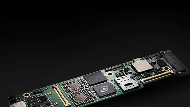
This began with last year’s launch of Lakefield, a hybrid processor for foldable and dual-screen PCs and other ultra-light form factors. Lakefield consists of two variants—the Intel Core i5-L16G7 and Intel Core i3-L13G4—and each comes with one Sunny Cove core for high-performance applications and four Tremont cores for low-power background applications.
These two core types are made with different manufacturing processes. The Sunny Cove core, which also serves as the basis for Intel’s Ice Lake CPU for laptops and servers, is made using Intel’s 10-nanometer process. Tremont, on the other hand, is based on 14nm and also serves as the foundation for the company’s latest Atom, Celeron and Pentium CPUs.
Intel plans to continue this hybrid core approach with Alder Lake, the code name for the company’s 12th-generation Core processors for PCs that are set to come out in the second half of 2021.
Alder Lake will rely on the successors to the Sunny Cove and Tremont cores—Golden Cove for high performance and Gracemont for low power, respectively—to optimize performance-per-watt.
Raja Koduri, Intel’s chief architect and leader of the Architecture, Graphics and Software Group, said last year that Intel is working on a next-generation hardware-guided schedular that will optimize Alder Lake to squeeze every ounce of performance out of each core. Beyond delivering great performance, Alder Lake will also be Intel’s “best performance-per-watt architecture,” he added.
“While Lakefield was tuned for battery life, in Alder Lake, we have advanced the hybrid architectures significantly with a focus on performance,” he said.
Foveros And EMIB Are Shaking Up How CPUs Are Made
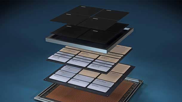
For decades, semiconductor companies embraced monolithic designs and made processors that fit everything onto a single die. But now companies are moving to a heterogenous approach and designing processors that are made up of chiplets, or in Intel’s case, tiles.
Intel is turning to this tile-based approach to “mix and match” different kinds of tiles for compute, graphics and AI, among other things, to optimize for performance and efficiency. These tiles can be made using different manufacturing processes, whether it’s on Intel’s internal fabs or those owned by external foundries like TSMC and Samsung.
Key to this approach are two emerging chip packaging technologies developed by Intel: Foveros for stacking tiles vertically across three layers and EMIB (embedded multi-die interconnect bridge) for integrating tiles horizontally on a single package.
During his IDM 2.0 presentation, Gelsinger said Foveros “is part of what gives us a really cool advantage in the next generation of our process road map, where we‘re going to be able to mix and match tiles from different process technologies but bring them together as if they were one single chip.”
The company’s Lakefield hybrid CPU from last year represented its first use of Foveros, which allowed Intel to make it dramatically smaller than other mobile processors. At roughly the size of a dime, Lakefield has a 56 percent smaller package area than an Intel Core i7-8500Y, giving OEMs more flexibility in designing innovative and small form factors like Lenovo’s ThinkPad X1 Fold.
Intel’s next CPU to use Foveros is Meteor Lake, a product for PCs due out in 2023 that will integrate tiles using different manufacturing processes as part of a modular design.
“This speaks to a larger industry transition as customers‘ needs and workloads diversify and grow in complexity,” Gelsinger said. “The world will move from system-on-a-chip to system-on-package, and Intel’s unquestioned leadership and packaging technologies become even more valuable. Being able to expertly construct the best products using the best technologies is a critical differentiator for us and one that delivers enormous value for our customers.”
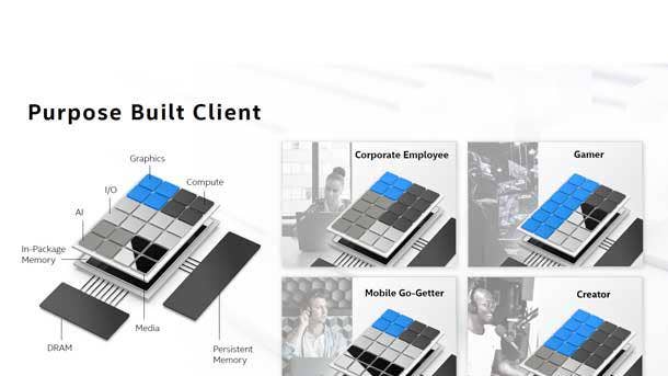
‘Client 2.0’ CPU Approach Will ‘Mix And Match’ Building Blocks
With Intel’s new tile-based method to making processors, the company plans to mix and match these tiles to create “purpose-built” CPUs for different user types, such as gamers, content creators and commercial users, as part of a new “Client 2.0” design approach.
For example, a processor for gamers could feature 12 graphics tiles, four compute tiles, four media tiles and four I/O tiles while a processor for corporate users could feature more AI and compute tiles and fewer graphics tiles. Intel also provided examples of purpose-built processors for content creators and people who travel a lot.
When the company teased the Client 2.0 approach last year, Brijesh Tripathi, vice president and chief technology officer for Intel‘s Client Computing Group, said it would allow for a much quicker development time than methods for designing monolithic and multi-die chips.
Tripathi said the quicker development time is made possible in part by the fact that the tiles for things like graphics, compute and I/O can be reused for different products at a much greater rate than dies used in multi-die chip architectures.
“Overall, Client 2.0 is about delivering winning products at an annual cadence,” he said.

Intel Is Turning To External Foundries For Some Top CPUs
As part of Intel’s new IDM 2.0 strategy, the company will ramp up its use of external foundries for products, including tiles for some of its top chips.
Previously, the company used external foundries to make chips for communications, connectivity, graphics and chipsets. But the new strategy means Intel will turn to foundries for top products the company had previously manufactured in-house. This includes modular tiles for server and client CPUs coming out in 2023 that will rely on TSMC, the same foundry used by its rival, AMD.
“The strength of our new IDM 2.0 model means we can strategically use the breadth of our ecosystem to our advantage,” Gelsinger said during Intel’s webcast on the new IDM 2.0 strategy last week. “For our 2023 road map, we will also leverage our relationship with TSMC to deliver additional leadership CPU products for our client and data center customers.”
Gelsinger said Intel will increase its use of not just TSMC but also Samsung, GlobalFoundries and UMC for manufacturing the company’s products, which will give the company “the increased flexibility and scale we need to optimize our road maps for cost, performance, schedule and supply.” This will create a “unique competitive advantage” for Intel, he added.
This means Intel will be able to take advantage of next-generation manufacturing processes developed by external foundries when they can provide a greater advantage on things like performance and cost over processes developed at Intel’s internal fabs.